Sunday 02 February 2025
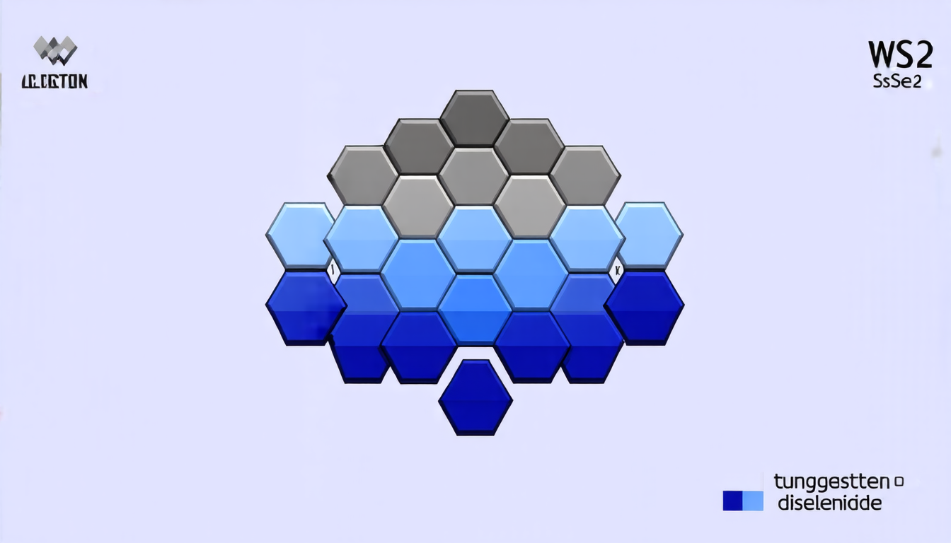
Researchers have made a significant breakthrough in understanding the behavior of charge carriers in two-dimensional materials, specifically in tungsten diselenide (WSe2). By using scanning tunneling microscopy (STM), scientists have been able to map the local density of states (LDOS) in WSe2 and observe how it changes as the material is subjected to different biases.
The LDOS is a measure of the probability of finding an electron at a given energy and location within the material. In WSe2, this probability is influenced by the material’s atomic structure and the way electrons interact with each other. By mapping the LDOS, researchers can gain insight into how charge carriers move through the material and how they respond to external influences.
In their study, scientists used STM to image the LDOS in WSe2 at different biases, ranging from -1.7 to -1.9 volts. They found that as the bias was increased, the LDOS changed significantly, with the probability of finding an electron shifting from the centers of the material’s hexagonal lattice cells to the edges.
This shift is attributed to the material’s unique atomic structure and the way electrons interact with each other. Specifically, researchers found that the material’s valence band has a non-trivial C3 eigenvalue, which means that it does not transform trivially under three-fold rotations. This property leads to the observed shift in the LDOS.
The results of this study have significant implications for our understanding of charge transport in two-dimensional materials. By better understanding how charge carriers move through these materials, researchers can design new devices and applications that take advantage of their unique properties.
One potential application of this research is in the development of quantum computing devices. WSe2 has been shown to exhibit quantum Hall effects, which could be harnessed for quantum computing purposes. By better understanding how charge carriers behave in this material, researchers may be able to improve the performance and efficiency of these devices.
Another area where this research may have an impact is in the development of new sensors and detectors. WSe2 has been shown to exhibit high sensitivity to changes in its environment, making it a promising candidate for use in sensors and detectors. By better understanding how charge carriers behave in this material, researchers may be able to improve the performance and accuracy of these devices.
In summary, researchers have made significant progress in understanding the behavior of charge carriers in WSe2 using STM.
Cite this article: “Unlocking the Secrets of Charge Transport in Tungsten Diselenide”, The Science Archive, 2025.
Tungsten Diselenide, Scanning Tunneling Microscopy, Local Density Of States, Charge Carriers, Two-Dimensional Materials, Atomic Structure, Electron Interaction, Valence Band, C3 Eigenvalue, Quantum Computing, Sensors And Detectors