Friday 14 March 2025
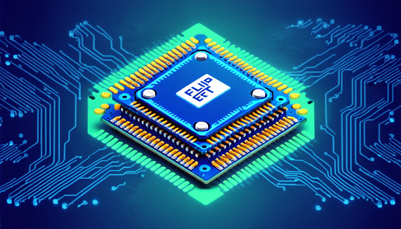
The latest advancements in technology have led to the development of a revolutionary new transistor architecture – the Flip FET (FFET). This innovative design combines the benefits of both 3D stacked transistors and fully functional backside power delivery networks, offering significant improvements over traditional logic devices.
One of the key challenges facing modern computing is the need for increased processing power while minimizing energy consumption. The FFET addresses this issue by leveraging its unique architecture to reduce power consumption and increase clock speeds. By stacking transistors vertically, the FFET can achieve higher packing densities than traditional planar transistors, allowing for more efficient use of space on silicon wafers.
In addition to its improved performance, the FFET also offers significant advantages in terms of design flexibility. The ability to place power delivery networks and signals on both sides of the chip allows for greater freedom in designing complex electronic systems. This flexibility can be particularly beneficial in applications where power consumption is critical, such as high-performance computing and artificial intelligence.
The development of the FFET has also led to the creation of a novel placement strategy that optimizes the distribution of power delivery networks and signals on both sides of the chip. This approach allows for more efficient use of space and reduced power consumption, further enhancing the overall performance of the device.
To test the capabilities of the FFET, researchers created a comprehensive evaluation framework that assesses its physical implementation and power-performance-area (PPA) characteristics. The results showed significant improvements in terms of area utilization, frequency, and power consumption compared to traditional logic devices.
One of the most impressive aspects of the FFET is its ability to maintain high levels of performance while reducing power consumption. In tests, the device achieved a 25% reduction in power consumption while maintaining a 12.5% increase in clock speed over traditional logic devices.
The FFET’s unique architecture also allows for greater flexibility in designing complex electronic systems. By placing power delivery networks and signals on both sides of the chip, designers can optimize their designs for specific applications, such as high-performance computing or artificial intelligence.
While the FFET is still a relatively new technology, its potential implications are vast. As computing continues to evolve, the need for more efficient and powerful logic devices will only continue to grow. The FFET’s innovative architecture and design flexibility make it an attractive solution for meeting these demands, and its impact on the field of electronics could be significant.
Cite this article: “Revolutionizing Logic Devices: The Flip FET (FFET) Architecture”, The Science Archive, 2025.
Transistors, Flip Fet, 3D Stacked Transistors, Power Delivery Networks, Logic Devices, Computing, Artificial Intelligence, High-Performance Computing, Silicon Wafers, Packing Densities