Wednesday 04 June 2025
Deep learning has revolutionized many fields, from image recognition to natural language processing. But what about manufacturing? A new study shows that a combination of deep learning and topological data analysis can be used to identify defects in semiconductor wafers more accurately than traditional methods.
Semiconductor wafers are the building blocks of modern electronics, powering everything from smartphones to computers. However, the process of producing these wafers is complex and prone to errors. Defects can occur at various stages, from raw material extraction to final assembly, causing costly rework or even complete product failure.
Traditional methods for detecting defects rely on manual inspection by human experts. But this approach has limitations – it’s time-consuming, labor-intensive, and prone to human error. Moreover, as the complexity of modern electronics increases, the number of possible defect patterns grows exponentially, making it increasingly difficult for humans to identify them.
That’s where deep learning comes in. By training artificial neural networks on large datasets of images of wafers with known defects, researchers have developed algorithms that can learn to recognize subtle patterns and anomalies. These algorithms can then be used to automatically inspect wafers and flag potential defects.
However, traditional deep learning approaches have limitations too. They often rely on handcrafted features or manual annotations, which can be time-consuming and costly to create. Moreover, they may not generalize well to new datasets or defect types.
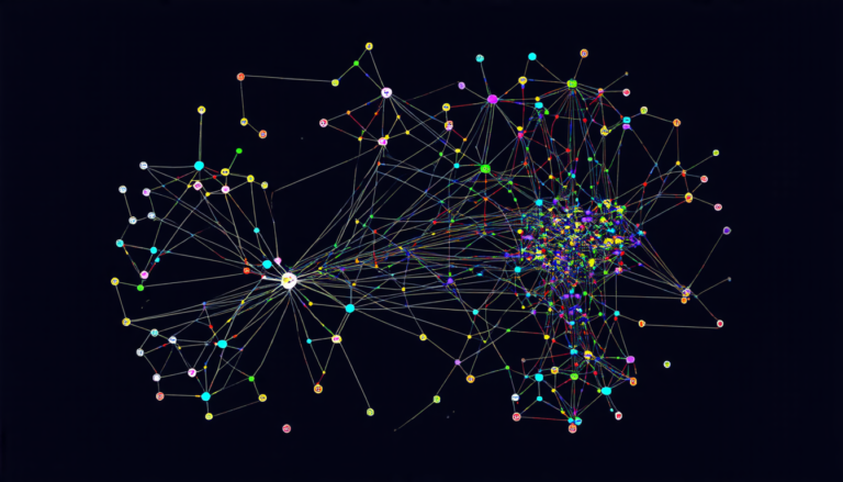
Enter topological data analysis (TDA). TDA is a mathematical framework that allows researchers to analyze complex data by focusing on the underlying structure of patterns and relationships rather than individual features. In the context of semiconductor wafer inspection, TDA can help identify defects by recognizing the way different patterns and anomalies are connected and interacting.
The new study combines deep learning with TDA to create a more powerful defect detection algorithm. By using TDA to extract meaningful features from large datasets of images, researchers can train neural networks that are better able to recognize subtle patterns and anomalies.
In practice, this means that the algorithm can identify defects more accurately and quickly than traditional methods. The study showed that the combined approach outperformed both human inspectors and traditional automated inspection systems in detecting defects.
The implications of this research are significant. By automating defect detection using deep learning and TDA, manufacturers can reduce costs, increase efficiency, and improve product quality. This could have a major impact on the entire electronics industry, from smartphone production to advanced manufacturing processes.
Cite this article: “Deep Learning Meets Topological Data Analysis: Accurate Defect Detection in Semiconductor Wafers”, The Science Archive, 2025.
Semiconductor Wafers, Deep Learning, Topological Data Analysis, Defect Detection, Artificial Neural Networks, Image Recognition, Natural Language Processing, Manufacturing, Electronics Industry, Automation