Thursday 27 February 2025
Scientists have made a significant breakthrough in understanding the behavior of nanowires, tiny structures that are just a few billionths of a meter in size. These tiny marvels have been gaining attention in recent years due to their potential applications in fields such as electronics and medicine.
Nanowires can be thought of as tiny tubes or wires that are made up of individual atoms arranged in a specific pattern. They can be grown using various techniques, including the use of chemical vapors and high-temperature furnaces. In this study, researchers focused on the growth of nanowires made from a combination of gallium arsenide (GaAs) and indium phosphide (InP).
The team used a technique called molecular beam epitaxy to grow the nanowires. This involves directing a beam of atoms onto a surface, allowing them to bond together and form a crystal structure. In this case, the researchers used beams of GaAs and InP atoms to create a core-shell structure, with the GaAs forming the central core and the InP forming a shell around it.
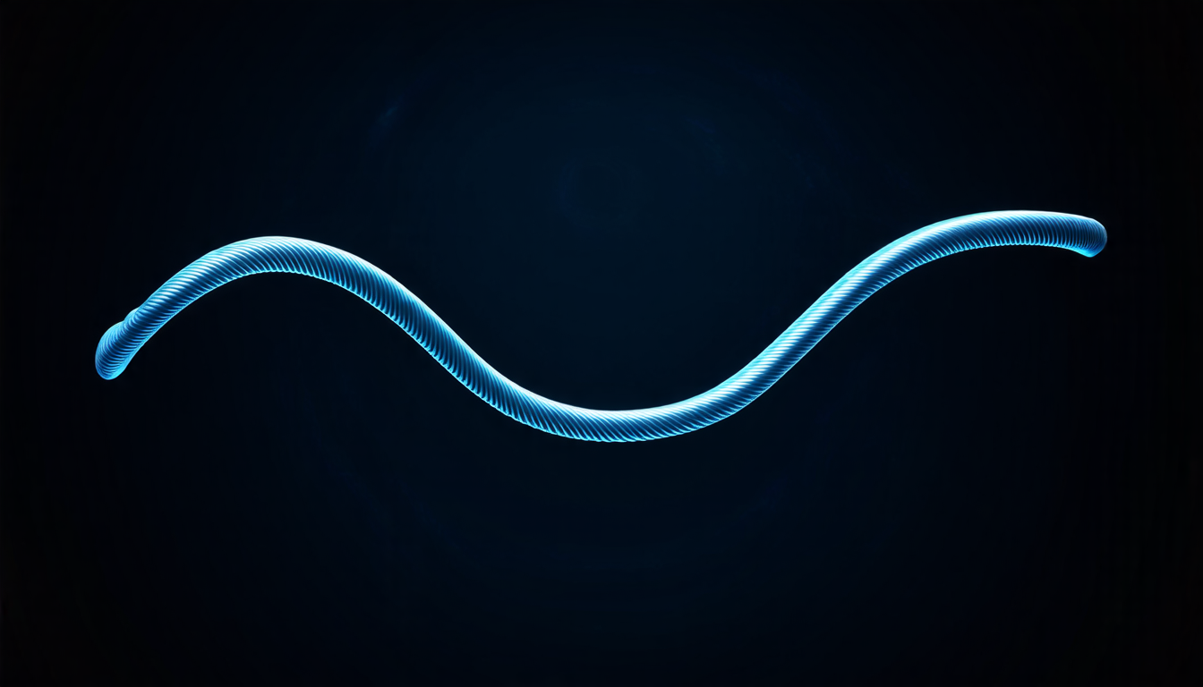
The resulting nanowires were found to exhibit unique properties, including the ability to bend and twist in specific ways. This is due to the different crystal structures of the GaAs and InP materials, which can cause stress and strain within the wire. By studying these behaviors, researchers hope to gain a better understanding of how nanowires interact with their environment.
One of the key findings of this study was that the orientation of the phosphorus beam used during growth had a significant impact on the properties of the resulting nanowire. The team found that when the beam was aligned in a specific way, the nanowire would bend and twist more significantly than if it were aligned differently.
This discovery has important implications for the development of new technologies, such as sensors and transistors. By understanding how to control the growth of nanowires and their properties, researchers may be able to create devices that are smaller, faster, and more efficient.
The study also highlights the importance of using advanced imaging techniques to analyze the structure and behavior of nanowires. The team used a technique called transmission electron microscopy (TEM) to visualize the internal structure of the nanowires and study their properties in detail.
Overall, this research has significant implications for our understanding of nanowire behavior and its potential applications in various fields.
Cite this article: “Unlocking the Secrets of Nanowires: A Breakthrough in Understanding Their Behavior”, The Science Archive, 2025.
Nanowires, Gaas, Inp, Molecular Beam Epitaxy, Core-Shell Structure, Crystal Structure, Stress, Strain, Transmission Electron Microscopy, Tem