
Thursday 06 March 2025
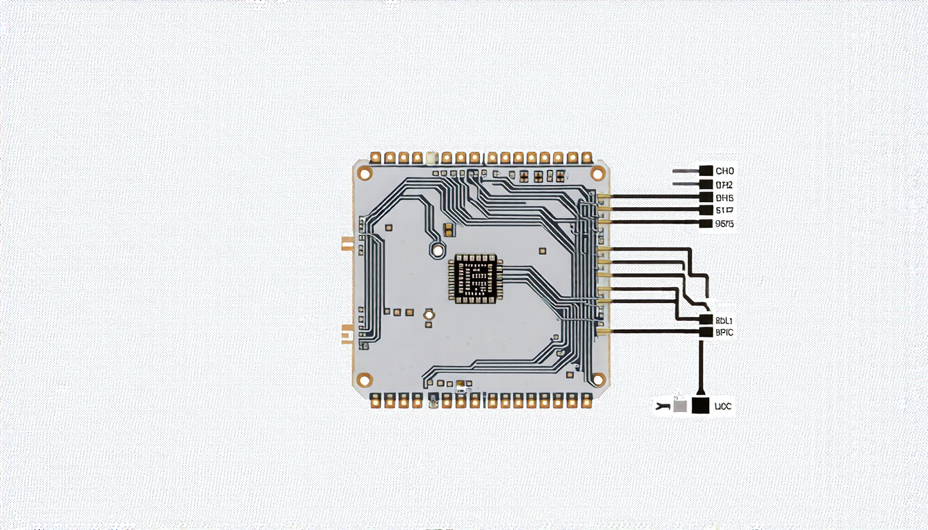
The quest for defect-free printed circuit boards (PCBs) has long been a holy grail of electronics manufacturing. With the increasing complexity of modern devices, ensuring that these tiny pieces of silicon-based magic are free from imperfections is no small feat. Enter the latest innovation in PCB inspection: GAN-enhanced YOLOv11.
For those unfamiliar with the jargon, YOLO (You Only Look Once) is a popular object detection algorithm that’s been making waves in computer vision circles. By leveraging convolutional neural networks and advanced image processing techniques, YOLO has proven itself to be a reliable tool for spotting defects on PCBs. However, as PCB designs become increasingly intricate, the need for more sophisticated inspection methods has grown.
Enter GAN (Generative Adversarial Network), a type of AI that’s specifically designed to generate realistic data. In this case, researchers have used GAN to create synthetic defect images that can be fed into YOLOv11 training. The result? A model capable of detecting even the most elusive imperfections with uncanny accuracy.
The key innovation here lies in the way GAN-generated defects are used to augment the training dataset. By incorporating these artificially created flaws, the model learns to recognize subtle patterns and shapes that might otherwise go undetected. This is particularly important when it comes to complex PCB designs, where small defects can have far-reaching consequences.
In practical terms, this means that manufacturers can now rely on YOLOv11 to identify issues like missing holes, mouse bites, open circuits, short circuits, burrs, and virtual welding with unprecedented precision. The implications are significant: by detecting these imperfections early in the manufacturing process, companies can reduce waste, streamline production, and ultimately deliver higher-quality products to customers.
But what about false positives? It’s a natural concern when introducing AI-powered inspection tools into the mix. Fortunately, the researchers behind this project have taken steps to mitigate this risk. By fine-tuning the model’s parameters and incorporating advanced loss functions, they’ve managed to reduce the number of false alarms to an acceptable level.
Of course, no inspection method is foolproof, and there are still limitations to be addressed. For instance, the GAN-generated defects may not perfectly replicate real-world imperfections, which could lead to some missed detections. However, as the researchers themselves acknowledge, this is a problem that can be addressed through further refinement of the model.
Cite this article: “AI-Powered PCB Inspection: A New Era in Defect Detection”, The Science Archive, 2025.
Printed Circuit Boards, Pcb Inspection, Gan-Enhanced Yolov11, Object Detection Algorithm, Convolutional Neural Networks, Image Processing, Defect Detection, Artificial Intelligence, Ai-Powered Inspection Tools, Electronics Manufacturing.