
Friday 14 March 2025
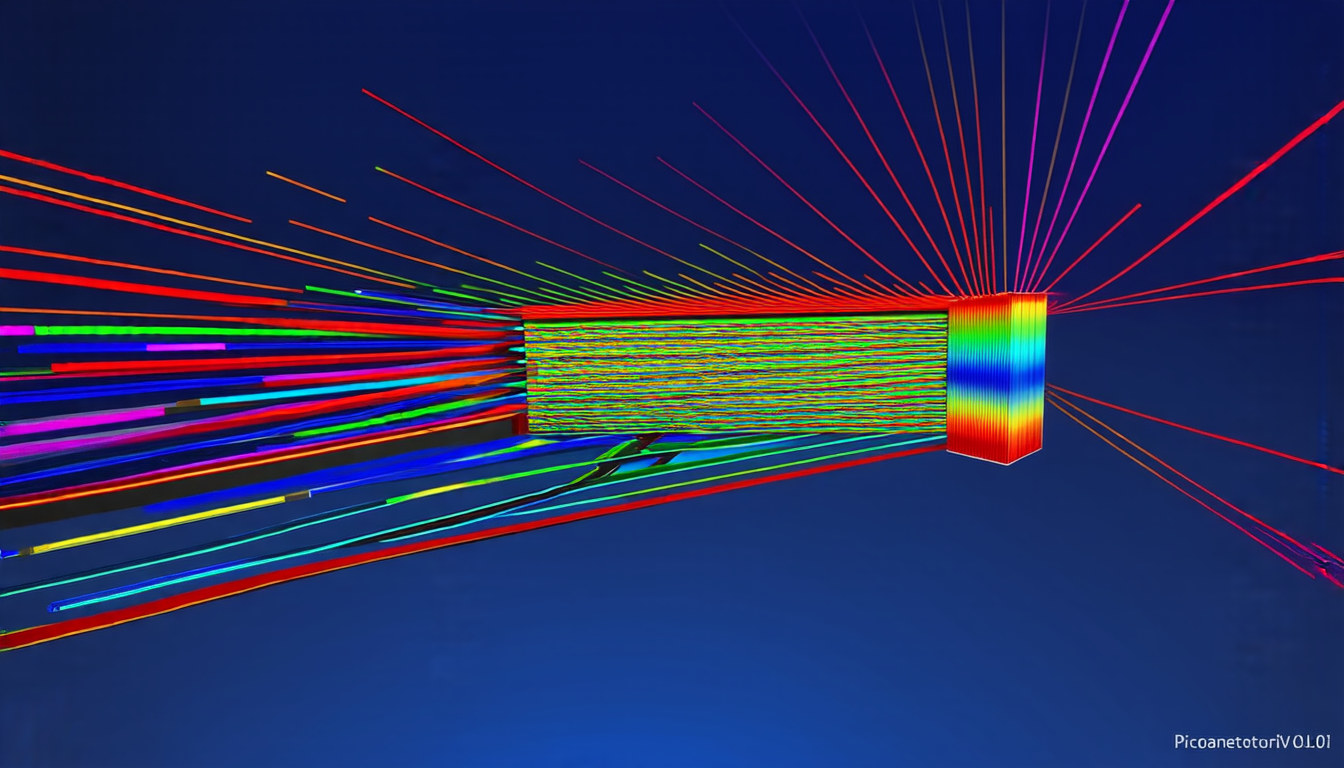
The latest advancements in the field of nanophotonics have brought us closer to creating compact and efficient on-chip wavelength demultiplexers, a crucial component for next-generation optical communication systems. Researchers have successfully designed and demonstrated an inverse-designed photonic demultiplexer that can sort and route distinct photoluminescence emissions from stacked transition metal dichalcogenide (TMDC) monolayers.
The TMDCs in question are WS2 and WSe2, which are known for their unique optical properties. When these materials are stacked together, they form a heterostructure that exhibits excitonic emission at specific wavelengths. The goal of this research was to create a device that can efficiently sort and route these emissions into separate channels.
To achieve this, the researchers employed an inverse design approach, which involves using optimization algorithms to discover optical structures based on desired functional characteristics. This allowed them to design a demultiplexer with a compact footprint of just 10 micrometers square.
The device consists of a thin layer of silicon nitride (Si3N4) on top of a quartz substrate, with patterned output channels that are designed to guide the photoluminescence emissions into separate channels. The researchers used finite-difference frequency domain simulations to optimize the design and verify its performance.
In experiments, the device was tested using laser light at 620 and 750 nanometers, as well as a tunable light source for excitation of the TMDCs. The results showed that the demultiplexer could efficiently sort and route the photoluminescence emissions into separate channels, with transmission efficiencies ranging from 69% to 87%.
The implications of this research are significant. On-chip wavelength demultiplexers have the potential to revolutionize optical communication systems by enabling faster and more efficient data transfer over long distances. The ability to compactly integrate these devices could also lead to the development of smaller and more portable optical communication systems.
One of the key advantages of this inverse-designed demultiplexer is its scalability. The researchers were able to fabricate the device using standard semiconductor manufacturing techniques, which means that it can be easily integrated into existing chip designs. This makes it an attractive option for a wide range of applications, from data centers and cloud computing systems to optical interconnects in high-performance computing.
Overall, this research represents a significant step forward in the development of compact and efficient on-chip wavelength demultiplexers.
Cite this article: “Compact Inverse-Designed Photonic Demultiplexer for Efficient Optical Communication”, The Science Archive, 2025.
Nanophotonics, Wavelength Demultiplexer, Tmdc, On-Chip, Optical Communication, Photoluminescence, Inverse Design, Silicon Nitride, Finite-Difference Frequency Domain, Compact Devices