Wednesday 19 March 2025
Scientists have made a significant breakthrough in the field of nanophotonics, allowing them to create highly efficient and tunable light-matter interactions. By manipulating the surface topography of two-dimensional materials, researchers have been able to engineer novel optical properties that could lead to the development of advanced optoelectronic devices.
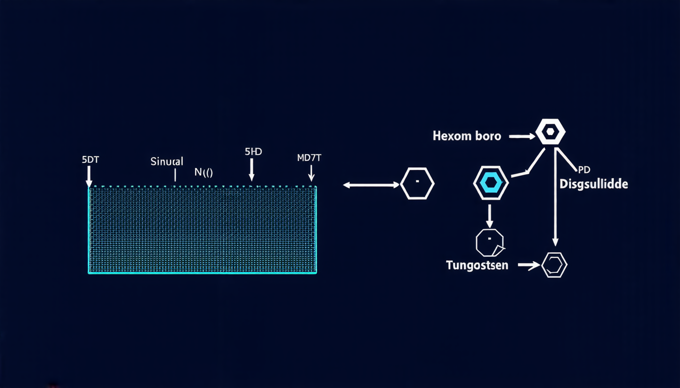
The team achieved this by creating a van der Waals heterostructure consisting of a layer of tungsten disulfide (WS2) embedded in hexagonal boron nitride (hBN). They then used thermal scanning-probe lithography to pattern a sinusoidal surface profile onto the top hBN layer. This unique structure allowed them to engineer the optical properties of the system, including the coupling strength between light and matter.
The researchers found that by tuning the spatial period and amplitude of the grating, they could control the energy of the excitonic resonance in the WS2 layer. They were also able to manipulate the waveguide modes in the hBN slab, allowing them to create a highly efficient system for generating polaritons.
Polaritons are hybrid particles that combine light and matter, and they have been shown to exhibit unique properties such as enhanced optical nonlinearity and ultra-slow group velocities. The ability to generate these particles on demand could lead to the development of advanced optoelectronic devices with applications in fields such as quantum computing, sensing, and communication.
The team’s findings were published in a recent paper, where they demonstrated the potential of their approach by measuring the angle-resolved reflectance spectra from the patterned hBN slab. They observed clear evidence of polariton formation, including the characteristic anti-crossing behavior that occurs when the excitonic resonance is tuned into resonance with the waveguide modes.
The results suggest that this novel approach could be used to develop highly efficient and tunable light-matter interactions, which would enable a wide range of applications in nanophotonics. The ability to engineer the optical properties of two-dimensional materials using thermal scanning-probe lithography opens up new possibilities for creating advanced optoelectronic devices with unique properties.
The researchers are already exploring ways to further optimize their approach and scale up the fabrication process. With continued advancements, this technology could lead to the development of compact and efficient light sources, high-speed optical switches, and even quantum computers that rely on the manipulation of polaritons.
Cite this article: “Engineering Polaritons in 2D Materials for Advanced Optoelectronics”, The Science Archive, 2025.
Nanophotonics, Light-Matter Interactions, Two-Dimensional Materials, Tungsten Disulfide, Hexagonal Boron Nitride, Van Der Waals Heterostructure, Thermal Scanning-Probe Lithography, Polaritons, Optoelect