
Thursday 20 March 2025
The quest for smaller, faster, and more efficient electronics has led scientists to explore the properties of two-dimensional (2D) materials. These materials are composed of a single layer of atoms, making them incredibly thin and strong. In recent years, researchers have been studying the behavior of 2D materials when combined with other materials in vertical heterostructures.
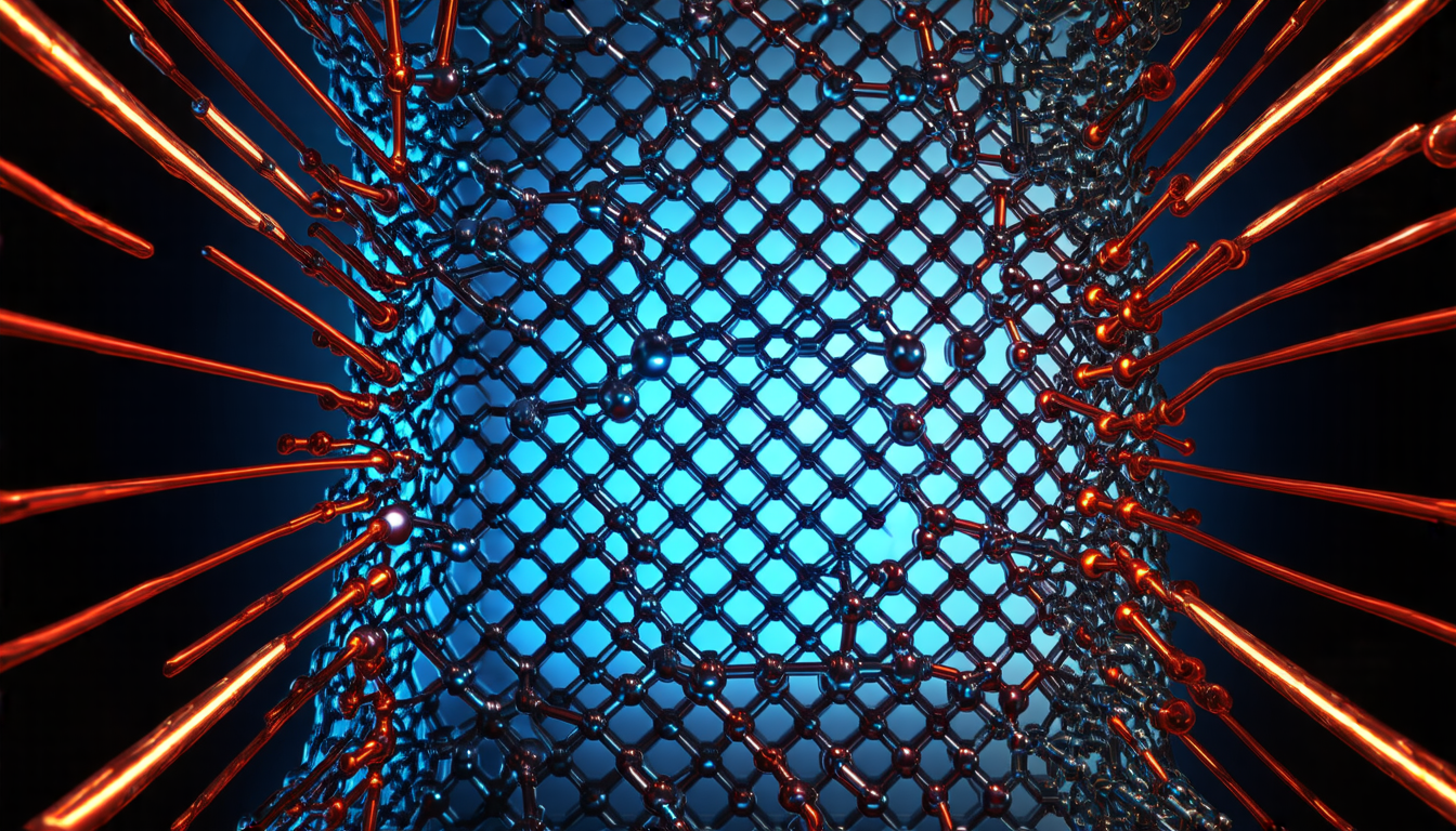
A new study published in a scientific journal has shed light on the electronic properties of these hybrid structures. By simulating various combinations of metal and 2D material interfaces, researchers have discovered that the electronic characteristics of the 2D material can be significantly altered by its interaction with the metallic electrodes.
In traditional electronics, electrons flow easily through metals due to their high conductivity. However, when a 2D material is placed between two metal electrodes, it behaves differently. The strong orbital hybridization between the metal atoms and the 2D material leads to the formation of new electronic states within the bandgap of the 2D material.
This phenomenon has significant implications for the development of novel electronic devices. For instance, researchers have found that a single layer of hexagonal boron nitride (hBN) can become conductive when placed between non-passivated metallic electrodes. This is unexpected, as hBN is typically an insulator in its isolated form.
The study also explored the behavior of trilayer structures, where three layers of 2D material are stacked together with metal electrodes at either end. In these cases, the middle layer retains its intrinsic electronic properties, while the top and bottom layers are strongly influenced by the metallic contacts.
The findings suggest that the choice of electrode material and the stacking configuration can significantly impact the electronic behavior of the 2D material. This knowledge can be used to design custom multilayer structures with tailored electrical properties for specific applications.
In addition to their potential use in electronics, these hybrid structures may also have implications for the development of future computing architectures. As devices become increasingly smaller and more complex, researchers are exploring new ways to integrate multiple layers and materials to achieve faster processing speeds and reduced power consumption.
The study’s results demonstrate the importance of understanding the interfacial properties between 2D materials and metal electrodes in the development of next-generation electronics. By continuing to explore these interactions, scientists may uncover new opportunities for innovation in fields such as computing, energy storage, and optoelectronics.
Cite this article: “Electronically Tuning 2D Materials with Metal Interfaces”, The Science Archive, 2025.
Two-Dimensional Materials, Hybrid Structures, Metal Electrodes, Electronic Properties, Bandgap, Conductivity, Insulators, Trilayers, Multilayer Structures, Computing Architectures.