Thursday 27 March 2025
The quest for efficiency in electronic design has led researchers to develop innovative solutions to optimize the placement of components on printed circuit boards (PCBs). A recent paper proposes a double-layer placement algorithm that tackles this challenge by modeling the problem as a mixed-variable optimization issue.
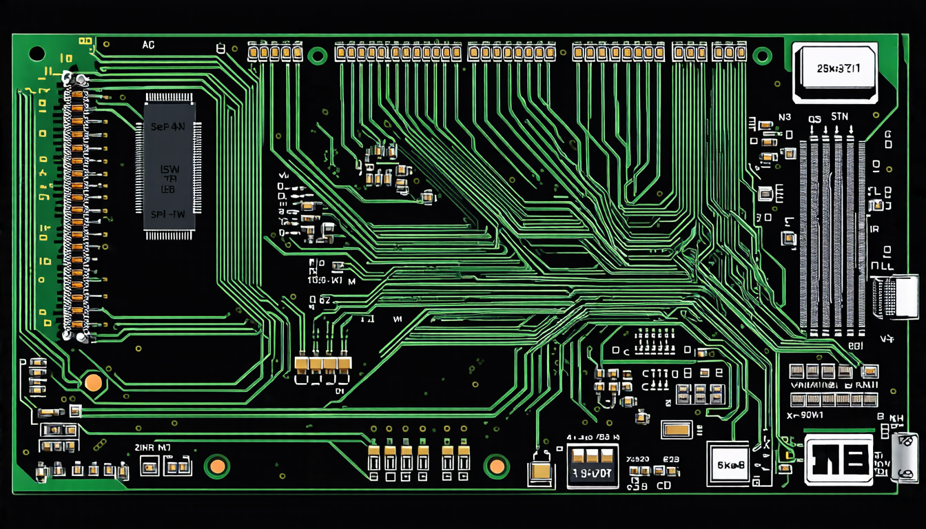
To understand the complexity of PCB design, consider a typical scenario: a board comprising various functional modules, such as integrated circuits (ICs), resistors, and capacitors. These components must be arranged in a way that minimizes wire length while respecting physical constraints like component size and pin orientation. The task is further complicated by the need to balance conflicting objectives, such as minimizing area usage and ensuring reasonable spacing between components.
The proposed algorithm addresses these challenges by dividing the placement problem into two subproblems: top-layer centralized placement and bottom-layer pin-oriented placement. The first subproblem focuses on placing ICs and other large modules in a way that reduces wire length and minimizes component movement during subsequent iterations. In contrast, the second subproblem involves arranging smaller components like resistors and capacitors around the ICs to optimize pin usage.
To solve these subproblems, the researchers employed tailored algorithms for global placement and legalization. The global placement strategy ensures an initial arrangement of components that satisfies design constraints while minimizing wire length. Legalization then refines this arrangement by eliminating overlaps and adjusting component positions to meet specific requirements like component size and pin orientation.
The algorithm’s performance was evaluated on various industrial PCB cases, showcasing its ability to efficiently place components with minimal movement. The results demonstrate a significant reduction in wire length compared to existing placement algorithms, making it an attractive solution for large-scale PCB designs.
One of the key strengths of this approach lies in its ability to handle diverse design scenarios by incorporating flexible legalization strategies. This adaptability allows the algorithm to accommodate different component sizes, shapes, and pin orientations, ultimately leading to more efficient placements.
Furthermore, the proposed algorithm’s scalability is noteworthy, as it can efficiently solve large-scale placement problems with millions of components. This capability makes it an attractive solution for modern electronics design, where PCBs often feature complex arrangements of components.
The paper’s findings have significant implications for the development of high-performance electronic systems. By optimizing component placement, designers can reduce wire length and increase system reliability, ultimately leading to more efficient and cost-effective designs. As the demand for advanced electronics continues to grow, innovative solutions like this algorithm will play a vital role in shaping the future of PCB design.
Cite this article: “Efficient Component Placement on Printed Circuit Boards through Double-Layer Algorithm”, The Science Archive, 2025.
Printed Circuit Boards, Electronic Design, Component Placement, Mixed-Variable Optimization, Wire Length Minimization, Pcb Design, Ics, Resistors, Capacitors, Legalization Strategies.